


Semiconductor Electronic Material Devices And Simple Circuits Class 12 important questions with answers PDF download
Semiconductor Electronics, Chapter 14 of Class 12 Physics, introduces the fascinating world of semiconductors, their properties, and applications. This chapter's important questions cover key concepts like diodes, transistors, and logic gates, forming the foundation of modern electronics. It emphasises practical applications in circuits and devices. Download the Class 12 Physics Syllabus for detailed coverage and explore our exclusive Class 12 Physics Important Questions PDF to solidify your understanding and crack your exams.
 Table of Content


1 Mark Questions
1. Give the ratio of number of holes and the number of conduction electrons in an intrinsic semiconductor.
Ans:
$\frac{{{n}_{h}}}{{{n}_{e}}}=1$ (In intrinsic semiconductor, ${{n}_{e}}={{n}_{h}}$).
2. What type of impurity is added to obtain n-type semiconductor?
Ans: Pentavalent atoms (group -$15$) like Phosphorus (P), Arsenic (As), etc.
3. Doping of silicon with indium leads to which type of semiconductor?
Ans: Doping of Silicon with Indium produces a p-type semiconductor as Indium is a trivalent impurity.
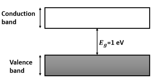
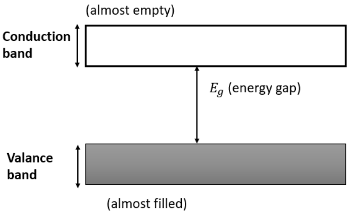
4. Draw an energy level diagram for an intrinsic semiconductor.
Ans:
In intrinsic semiconductor, ${{n}_{e}}={{n}_{h}}$
The energy level diagram for an intrinsic semiconductor is shown below:
5. A semiconductor has equal electron and hole concentration of $6\times {{10}^{8}}{{m}^{-3}}$. On doping with a certain impurity electron concentration increases to $3\times {{10}^{12}}{{m}^{-3}}$. Identify the type of semiconductor after doping.
Ans:
According to the question, after doping, ${{n}_{e}}>{{n}_{h}}$.
Clearly, we get an n-type semiconductor after doping.
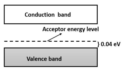
6. How does the energy gap of an intrinsic semiconductor vary, when doped with a trivalent impurity?
Ans: An acceptor energy level is formed in the forbidden energy gap above the valence band when an intrinsic semiconductor is doped with a trivalent impurity.
Due to this, electrons quickly jump to the acceptor energy level.
7. How does the width of the depletion layer of p-n-junction diode change with decrease in reverse bias?
Ans: The width of the depletion layer will decrease with decrease in reverse bias.
8. Under what condition does a junction diode work as an open switch?
Ans: A junction diode works as an open switch when it is connected under reverse bias conditions.
9. Which type of biasing gives a semiconductor diode very high resistance?
Ans: Reverse biasing gives a semiconductor diode very high resistance.
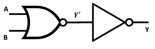
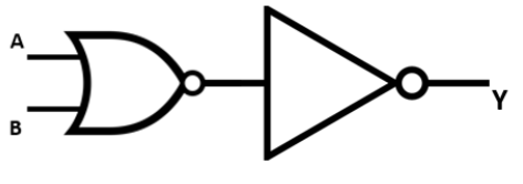
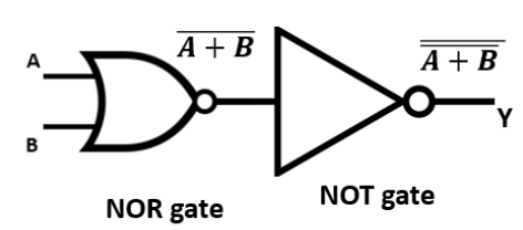
10. If the output of a 2-input NAND gate is fed as the input to a NOT gate,
a) name the new logic gate obtained and
Ans:
An AND gate is obtained when the output of a 2-input NAND gate is fed as the input to a NOT gate.
b) write down its truth table
Ans:
Truth table for an AND gate is given below.
11. Define current amplification factor in a common – emitter mode of transistor.
Ans: Current amplification factor is the fraction of a small change in collector current to the slight difference in base current at constant collector-emitter junction voltage.
12. Why is a semiconductor damaged by a strong current?
Ans: When a strong current traverses through a semiconductor, a large amount of heat is generated, which breaks the covalent links in the semiconductor. This causes the semiconductor to get damaged.
2 Marks Questions
1. Draw a p-n junction with reverse bias. Which biasing will make the resistance of a p-n-junction high?
Ans: The diagram of a p-n junction with reverse bias is as follows:
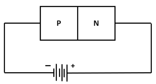
Reverse biasing will provide a high resistance and thus, will not permit the current to pass through the junction.
2. Write the truth table for the following combination of gates.
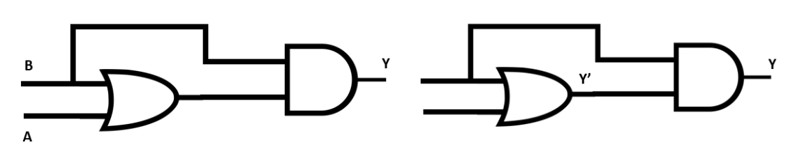
Ans:
Truth table for the given combination of gates is as follows:
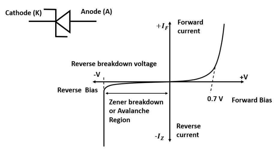
3. Draw the voltage current characteristics of a Zener diode.
Ans:
The voltage current characteristics of a Zener diode is as follows:
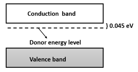
4. For an extrinsic semiconductor, indicate on the energy band diagram the donor and acceptor levels.
Ans: There are two types of extrinsic semiconductors: n-type extrinsic semiconductor and p-type extrinsic semiconductor. The energy band diagrams with the donor and acceptor levels are shown below:
5. What do you mean by depletion region and potential barrier in junction diode?
Ans: A layer around the intersection between p and n sections of a junction diode where charge carriers, electrons and holes are less in number is called the depletion region.
The potential difference created due to the diffusion of charge carriers across the junction is called the potential barrier.
6. A transistor has a current gain of $30$. If the collector resistance is $6k\Omega $, input resistance is $1k\Omega $, calculate its voltage gain.
Ans:
Given that:
${{R}_{in}}=1k\Omega $
${{R}_{out}}=6k\Omega $
$\therefore {{R}_{gain}}=\frac{{{R}_{out}}}{{{R}_{in}}}=\frac{6}{1}=6$
We also know that $\text{Voltage gain = current gain }\times \text{ }{{\text{R}}_{\text{gain}}}$
Clearly, voltage gain$=30\times 6=180$
7. What are the advantages and disadvantages of semiconductor devices over vacuum tubes?
Ans:
Advantages:
Semiconductor devices are tiny in size as compared to vacuum tubes.
They need low voltage for their operation.
Disadvantages:
On the application of high voltage as well as increase in temperature, semiconductors can be damaged easily.
8. The base of a transistor is lightly doped. Explain why?
Ans: In a transistor, most carriers from the emitter region move towards the collector region through the base.
If the base is made thick and highly doped, most carriers will combine with the other carriers within the base, and only a few are collected by the collector, leading to a small output collector current.
Thus, to have a large output collector current, the base is made thin and lightly doped.
9. When similar diodes ${{D}_{1}}$ and ${{D}_{2}}$ are connected as shown, determine the currents through resistance $R$ of the circuits
a)
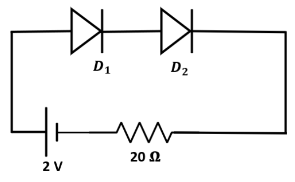
Ans:
In figure (i), ${{D}_{1}}$ and ${{D}_{2}}$ are forward biased.
$\Rightarrow I=\frac{V}{R}=\frac{2}{20}=0.1A$
b)
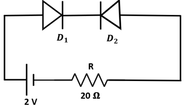
Ans:
In figure (ii), ${{D}_{1}}$ is forward biased but ${{D}_{2}}$ is reverse biased, due to which they provide infinite resistance.
$\Rightarrow I=0$ in this case.
10. What do you mean by hole in a circuit? Write its two characteristics.
Ans: A vacancy formed in a covalent bond in a semiconductor due to the release of an electron is known as a hole in a semiconductor.
Characteristics of hole are:
a) The hole is equivalent to a positive electric charge.
b) The mobility of a hole is smaller than that of an electron.
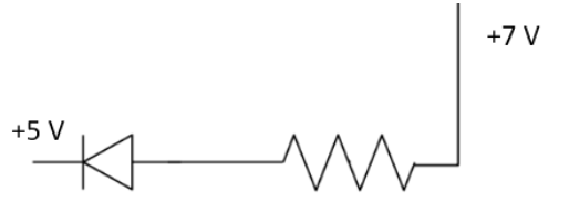
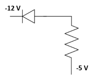
11. Diode used in the figure has constant voltages drop at $0.5V$ at all currents and a maximum power rating of $100mW$. What should be the value of the resistance $R$, connected in series for maximum current?
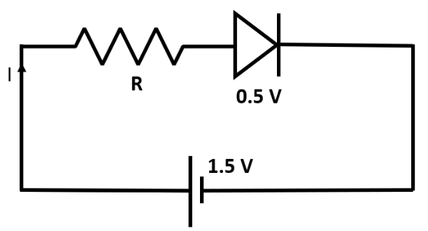
Ans:
It is given that:
$P=100mW=100\times {{10}^{-3}}$
$V=0.5V$
$P=VI$
$\Rightarrow I=\frac{P}{V}=\frac{100\times {{10}^{-3}}}{0.5}$
$I=0.2A$
For the given circuit, applying Kirchhoff’s rules,
$IR+0.5-1.5=0$
$IR=1$
$0.2\times R=1$
$R=\frac{1}{0.2}=5\Omega $
$R=5\Omega $
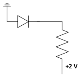
12. Zener diode has saturation current of $20A$ and reverse breakdown voltage of $100V$ whereas the corresponding value of are $40\mu A$ and \[40V\]. Find the current through the circuit.
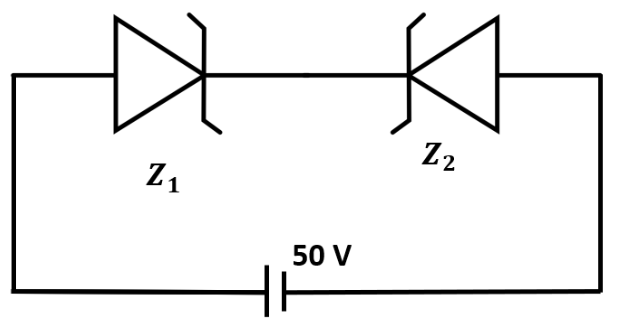
Ans:
Here, ${{Z}_{1}}$ is in forward biased whereas ${{Z}_{2}}$ is in reverse biased.
Clearly, ${{Z}_{1}}$ acts as a conductor and reverse saturation current will move from ${{Z}_{2}}$.
Thus,
${{R}_{{{Z}_{2}}}}=\frac{40}{40\times {{10}^{-6}}}$
${{R}_{{{Z}_{2}}}}={{10}^{6}}\Omega $
Now, $50V$ will appear across ${{Z}_{2}}$.
So, current
$I=\frac{50}{{{10}^{6}}}$
$I=50\times {{10}^{-6}}A$
13. In an n-type Silicon, which of the following statement is true?
a) Electrons are majority carriers and trivalent atoms are the dopants.
b) Electrons are minority carriers and pentavalent atoms are the dopants.
c) Holes are minority carriers and pentavalent atoms are the dopants.
d) Holes are majority carriers and trivalent atoms are the dopants.
Ans:
The correct statement is (c).
In an n-type Silicon, the majority carriers are electrons while the minority carriers are the holes.
When pentavalent atoms, such as Phosphorus are doped with Silicon atoms, an n-type semiconductor is obtained.
14. Which of the statements given in Question 13 is true for p-type semiconductors?
Ans:
The correct statement is (d).
In an p-type silicon, the majority carriers are holes while the minority carriers are the electrons.
When trivalent atoms, such as Aluminium are doped in Silicon atoms, a p-type semiconductor is obtained.
15. Carbon, Silicon and Germanium have four valence electrons each. These are characterised by valence and conduction bands separated by energy band gap respectively equal to \[{{({{E}_{g}})}_{C}},{{({{E}_{g}})}_{Si}}\] and ${{({{E}_{g}})}_{Ge}}$. Which of the following statements is true?
a) ${{({{E}_{g}})}_{Si}}<{{({{E}_{g}})}_{Ge}}<{{({{E}_{g}})}_{C}}$
b) ${{({{E}_{g}})}_{C}}<{{({{E}_{g}})}_{Ge}}>{{({{E}_{g}})}_{Si}}$
c) ${{({{E}_{g}})}_{C}}>{{({{E}_{g}})}_{Si}}>{{({{E}_{g}})}_{Ge}}$
d) ${{({{E}_{g}})}_{C}}={{({{E}_{g}})}_{Si}}={{({{E}_{g}})}_{Ge}}$
Ans:
The correct statement is (c).
Out of the three given elements, the energy band gap of Carbon is the maximum, and Germanium's energy band gap is the minimum.
The energy band gaps of the given elements have the relation:
${{({{E}_{g}})}_{C}}>{{({{E}_{g}})}_{Si}}>{{({{E}_{g}})}_{Ge}}$
16. In an unbiased p-n junction, holes diffuse from the p-region to n-region because
a) Free electrons in the n-region attract them.
b) They move across the junction by the potential difference.
c) Hole concentration in p-region is more as compared to n-region.
d) All the above.
Ans:
The correct statement is (c).
The movement of charge carriers across a junction takes place from higher concentration to lower concentration.
In this case, the p-region has a higher concentration of holes than the n-region. Hence, in an unbiased p-n junction, holes move from the p-region to the n-region.
17. When a forward bias is applied to a p-n junction, it
a) raises the potential barrier.
b) reduces the majority carrier current to zero.
c) lowers the potential barrier.
d) None of the above.
Ans:
The correct statement is (c).
When a p-n junction is forward biased, it reduces the value of the potential barrier. In the case of forward bias, the potential barrier reverses the applied voltage. Therefore, the potential barrier across the junction gets decreased.
18. For transistor action, which of the following statements are correct?
a) Base, emitter and collector regions should have similar size and doping concentrations.
b) The base region must be very thin and lightly doped.
c) The emitter junction is forward biased and collector junction is reverse biased.
d) Both the emitter junction as well as the collector junction are forward biased.
Ans:
The correct statements are (b) and (c).
For smooth action of transistor, the base region needs to be lightly doped and very thin.
Also, the emitter junction should be forward-biased whereas the collector junction should be reverse-biased.
19. For a transistor amplifier, the voltage gain
a) remains constant for all frequencies.
b) is high at high and low frequencies and constant in the middle frequency range.
c) is low at high and low frequencies and constant at mid frequencies.
d) None of the above.
Ans:
The correct statement is (c).
The transistor amplifier's voltage gain is constant at the mid-frequency range only. It is low at high and low frequencies.
20. In half-wave rectification, what is the output frequency if the input frequency is$50Hz$? What is the output frequency of a full-wave rectifier for the same input frequency?
Ans:
Given that:
Input frequency $=50Hz$.
For a half-wave rectifier, the output frequency and the input frequency are equal.
Therefore, output frequency for a half wave rectifier $=50Hz$.
For a full-wave rectifier, the output frequency is the twice of the input frequency.
Therefore, output frequency for a full wave rectifier $~=2\times 50=100Hz$.
3 Marks Questions
1. What is an ideal diode? Draw the output wave form across the load resistor $R$, if the input waveform is as shown in the figure.
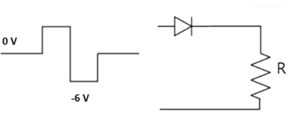
Ans:
An ideal diode provides zero resistance when it is forward biased and it offers an infinite resistance when it is reverse biased.
Output wave form across the load resistor $R$ for the given input waveform is
2. With the help of a labelled circuit diagram, explain full wave rectification using junction diode. Draw input and output wave forms.
Ans:
A full-wave rectifier comprises two diodes and a transformer with a central tap.
For any half cycle of AC input, only one diode is forward biased whereas the other one is reverse biased.
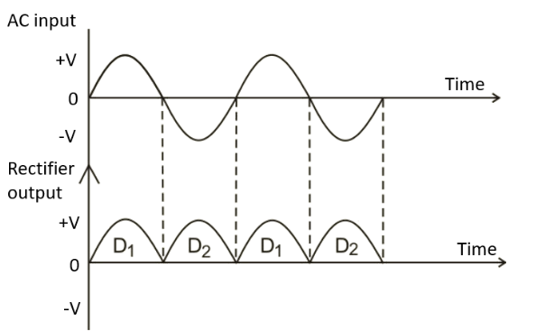
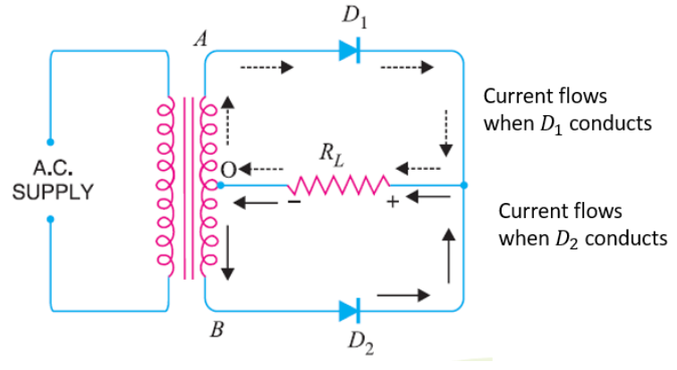
For positive half of AC input, diode ${{D}_{1}}$ is forward biased and ${{D}_{2}}$ is reverse biased, then the current will move across ${{D}_{1}}$ whereas for negative half of AC input, diode ${{D}_{2}}$ is forward biased and the current moves across ${{D}_{2}}$.
Thus, for both the half waves, output is obtained and the current moves in the same direction across load resistance ${{R}_{2}}$ and thus AC voltage is converted into DC.
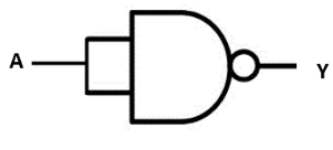
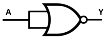
3. Name the gate shown in the figure and write its truth table?
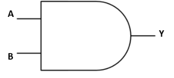
Ans:
The given gate is an AND gate and its truth table is:
4. In the following diagrams indicate which of the diodes are forward biased and which are reverse bias?
a)
Ans:
It is forward biased because cathode is connected to higher potential so, current will move from p to n.
b)
Ans.
It is reverse biased because cathode is grounded and n is connected with higher potential so, current will flow from n to p.
c)
Ans:
It is forward biased because cathode is connected to higher potential so, current will move from p to n.
5. In the given figure, is
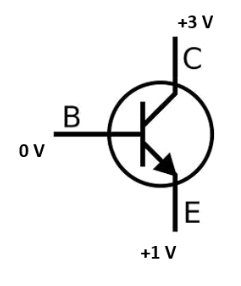
i. the emitter base is forward or reverse biased?
Ans.
Figure shows n-p-n transistor.
The emitter is reversed biased because the n-region is connected to a higher potential.
ii. collector base forward or reverse biased? Justify.
Ans:
The collector is also reversed biased because the n-region of the p-n junction is at a higher potential than the p-region.
6. Two semiconductor materials A and B shown in the figure are made by doping germanium crystal with arsenic and indium respectively. The two are joined end to end and connected to a battery as shown.
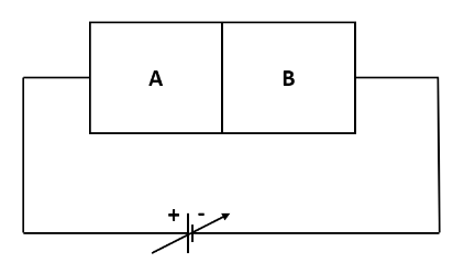
a) Will the junction be forward biased or reverse biased? Justify.
Ans:
Material A is n-type as it is doped with a pentavalent impurity and material B is p-type as it is doped with a trivalent impurity.
As a result, the junction becomes reverse biased because the battery's positive terminal is attached to the n-type and the battery's negative terminal is connected to the p-type. Hence it is reversed biased.
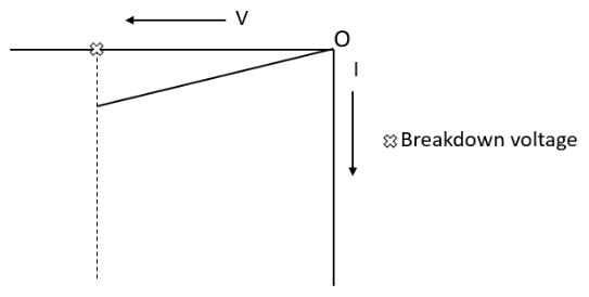
b) Sketch a V-I graph for this arrangement.
Ans.
V-I graph for the given circuit is given by:
7. Calculate emitter current for which $\beta =100$ and ${{I}_{B}}=20\mu A?$
Ans:
Given:
$\beta =100$,
${{I}_{B}}=20\mu A=20\times {{10}^{-6}}A$
$\beta =\frac{{{I}_{C}}}{{{I}_{B}}}$
${{I}_{C}}=\beta {{I}_{B}}=100\times 20=2000\mu A$
Using ${{I}_{E}}={{I}_{B}}+{{I}_{C}}$
\[{{I}_{E}}=20\times {{10}^{-6}}+2000\mu A\]
${{I}_{E}}=2020\mu A$
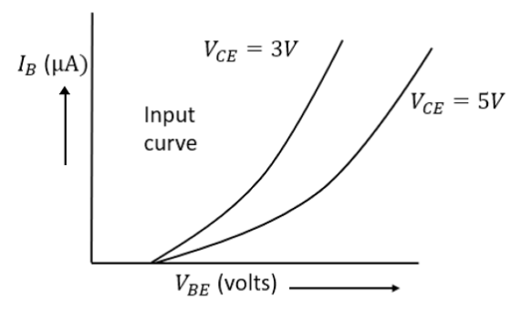
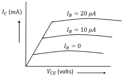
8. Draw the circuit diagram for common – emitter transistor characteristics using N-P-N transistor. Draw the input and output characteristic curve.
Ans:
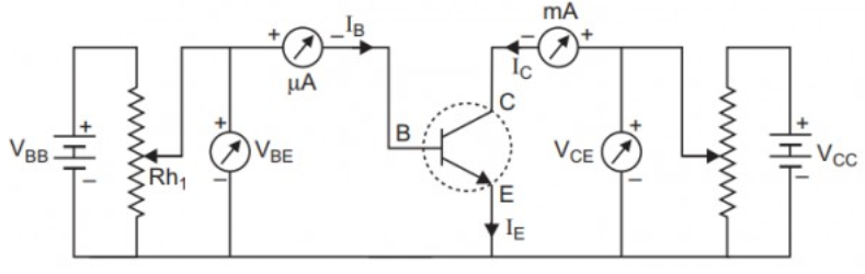
Input characteristic curve gives the base current variation ${{I}_{B}}$(Input) with base – emitter voltage (${{V}_{EB}}$) at fixed collector emitter voltage $({{V}_{CE}})$.
Output characteristic curve gives the collector current variation $({{I}_{C}})$ with collector emitter voltage $({{V}_{CE}})$ at fixed base current $({{I}_{B}})$.
9. For a CE-transistor amplifier, the audio signal voltage across the collected resistance of $2k\Omega $ is $2V$. Suppose the current amplification factor of the transistor is $100$, find the input signal voltage and base current, if the base resistance is $1k\Omega $.
Ans:
Collector resistance, ${{R}_{C}}=2k\Omega =2000\Omega $
Voltage across the collector resistance, $V=2V$
Current amplification factor of the transistor, $\beta =100$
Base resistance, ${{R}_{B}}=1k\Omega =1000\Omega $
Input signal voltage $={{V}_{i}}$
Base current $={{I}_{B}}$
Voltage amplification$=\frac{V}{{{V}_{i}}}=\beta \frac{{{R}_{C}}}{{{R}_{B}}}$
$\Rightarrow {{V}_{i}}=\frac{V{{R}_{B}}}{\beta {{R}_{C}}}$
$\Rightarrow {{V}_{i}}=\frac{2\times 1000}{100\times 2000}=0.01V$
Therefore, the input signal voltage of the amplifier is $0.01V$ .
Base current is given as:
${{I}_{B}}=\frac{{{V}_{i}}}{{{R}_{B}}}$
$\Rightarrow {{I}_{B}}=\frac{0.01}{1000}=10\times {{10}^{-6}}A$
Therefore, the base current of the amplifier is $10\mu A$ .
10. Two amplifiers are connected one after the other in series (cascaded). The first amplifier has a voltage gain of $10$ and the second has a voltage gain of $20$. If the input signal is $0.01$ volt, calculate the output ac signal.
Ans:
Given:
Voltage gain of the first amplifier, ${{A}_{{{V}_{1}}}}=10$
Voltage gain of the second amplifier, ${{A}_{{{V}_{2}}}}=20$
Input signal voltage, ${{V}_{i}}=0.01V$
Output AC signal voltage $={{V}_{0}}$
The total voltage gain of a two-stage cascaded amplifier is given by the product of voltage gains of both the stages, i.e.,
${{A}_{V}}={{A}_{{{V}_{1}}}}\times {{A}_{{{V}_{2}}}}$
$\Rightarrow {{A}_{V}}=10\times 20=200$
We have the relation:
${{A}_{V}}=\frac{{{V}_{0}}}{{{V}_{i}}}$
$\Rightarrow {{V}_{0}}={{A}_{V}}\times {{V}_{i}}$
$\Rightarrow {{V}_{0}}=200\times 0.01=2V$
Therefore, the output AC signal of the given amplifier is $2V$.
11. A p-n photodiode is fabricated from a semiconductor with band gap of $2.8eV$. Can it detect a wavelength of \[6000nm\]?
Ans:
Energy band gap of the given photodiode, ${{E}_{g}}=2.8eV$
Wavelength, $\lambda =6000nm=6000\times {{10}^{-9}}m$
The energy of a signal is given by the relation:
$E=\frac{hc}{\lambda }$
Where, $h=$ Planck’s constant
\[h=6.626\times {{10}^{-34}}Js\]
\[c=\text{speed of light}\]
\[c=3\times {{10}^{8}}m{{s}^{-1}}\]
$E=\frac{6.626\times {{10}^{-34}}\times 3\times {{10}^{8}}}{6000\times {{10}^{-9}}}$
$E=3.313\times {{10}^{-20}}J$
But $1.6\times {{10}^{-19}}J=1eV$
$\therefore E=3.313\times {{10}^{-20}}J=\frac{3.313\times {{10}^{-20}}}{1.6\times {{10}^{-19}}}=0.207eV$
The energy of a signal of wavelength $6000nm$ is $0.207eV$. It is less than $2.8eV$, which is the energy band gap of a photodiode. Hence, the photodiode cannot detect the signal.
12. The number of Silicon atoms per ${{m}^{3}}$ is $5\times {{10}^{28}}$ . This is doped simultaneously with $5\times {{10}^{22}}$ atoms per ${{m}^{3}}$of Arsenic and $5\times {{10}^{20}}$ per ${{m}^{3}}$ atoms of Indium. Calculate the number of electrons and holes. Given that ${{n}_{i}}=1.5\times {{10}^{16}}{{m}^{3}}$. Is the material n-type or p-type?
Ans:
Number of silicon atoms, $N=5\times {{10}^{28}}\text{atoms }{{\text{m}}^{\text{-3}}}$
Number of arsenic atoms, ${{n}_{As}}=5\times {{10}^{22}}\text{atoms }{{\text{m}}^{\text{-3}}}$
Number of indium atoms, ${{n}_{In}}=5\times {{10}^{20}}\text{atoms }{{\text{m}}^{\text{-3}}}$
Number of thermally-generated electrons, ${{n}_{i}}=1.5\times {{10}^{16}}\text{electrons }{{\text{m}}^{\text{-3}}}$
Number of electrons, ${{n}_{e}}=5\times {{10}^{22}}-\text{1}\text{.5}\times \text{1}{{\text{0}}^{16}}\approx 4.99\times {{10}^{22}}$
Number of holes $={{n}_{h}}$
In thermal equilibrium, the concentrations of electrons and holes in a semiconductor are related as:
${{n}_{e}}{{n}_{h}}=n_{i}^{2}$
$\Rightarrow {{n}_{h}}=\frac{{{(1.5\times {{10}^{16}})}^{2}}}{4.99\times {{10}^{22}}}\approx 4.51\times {{10}^{9}}$
Therefore, the number of electrons is approximately \[4.99\times {{10}^{22}}\] and the number of holes is about \[4.51\times {{10}^{9}}\].
Since the number of electrons (${{n}_{e}}$) is more than the number of holes (${{n}_{h}}$), the material is an n-type semiconductor.
13. Write the truth table for a NAND gate connected as given in Fig. 14.45.
Hence identify the exact logic operation carried out by this circuit.
Ans:
$A$acts as the two inputs of the NAND gate and $Y$ is the output, as shown in the following figure.
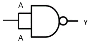
Hence, the output will be:
\[Y=\overline{A.A}=\bar{A}+\bar{A}=\bar{A}\] …… (i)
The truth table for equation (i) can be drawn as:
This circuit acts as a NOT gate. The symbol for this logic circuit is shown as:
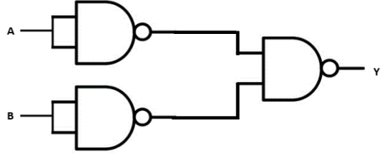
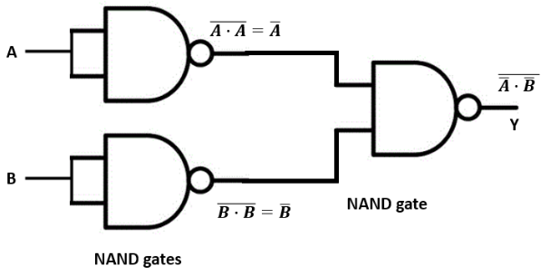
14. You are given two circuits as shown in Fig. 14.46, which consist of NAND gates. Identify the logic operation carried out by the two circuits.
a)
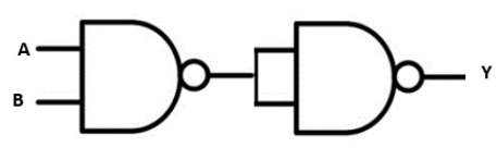
Ans:
In the given circuit, $A$ and $B$ are the inputs and $Y$ is the output.
The output of the first NAND gate will be $\overline{A.B}$ , as shown in the following figure.
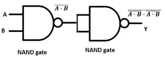
Clearly, the output of the combination of the two NAND gates is given as:
$Y=\overline{(\overline{A.B}).(\overline{A.B})}=\overline{\overline{A.B}}+\overline{\overline{A.B}}=A.B$
Hence, this circuit acts as an AND gate.
b)
Ans.
In the given circuit, $A$ and $B$ are the inputs and $Y$ is the output.
$\bar{A}$ is the output of the upper left NAND gate and \[\overline{B}\] is the output of the lower left NAND gate, as shown in the following figure.
Hence, the output of the combination of the NAND gates will be given as:
\[Y=\overline{\overline{A}.\overline{B}}=\overline{\overline{A}}+\overline{\overline{B}}=A+B\]
Clearly, this circuit acts as an OR gate.
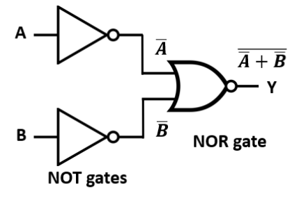
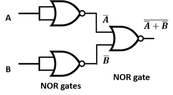
15. Write the truth table for circuit given in Fig. 14.47 below consisting of NOR gates and identify the logic operation (OR, AND, NOT) which this circuit is performing.
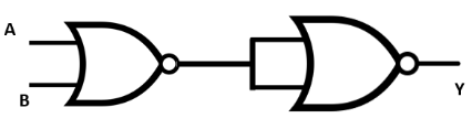
Ans:
$A$ and $B$ are the inputs of the given circuit.
The output of the first NOR gate is$\overline{A+B}$ .
It is observed from the given figure that the output of first NOR gate is the input of the second NOR gate.
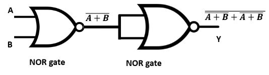
Hence, the output of the combination is given as:
$Y=\overline{\overline{A+B}+\overline{A+B}}=\overline{\overline{A}.\overline{B}}+\overline{\overline{A}.\overline{B}}$
$\Rightarrow Y=\overline{\overline{A}.\overline{B}}=\overline{\overline{A}}+\overline{\overline{B}}=A+B$
The truth table for this operation is given as:
This is the truth table of an OR gate. Hence, this circuit acts as an OR gate.
5 Marks Questions
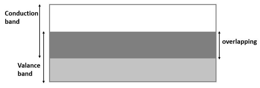
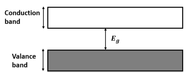
1. Distinguish between conductors, insulators and semiconductors on the basis of energy band diagrams.
Ans:
Conductor – The conduction band in a conductor is either partially filled, or the conduction and valence band overlap each other. There is no energy gap in a conductor.
Insulators – The conduction band and valence band of all insulators are widely separated by an energy gap of the order about \[6eV\] to \[9eV\]. Also, the conduction band of an insulator is almost empty.
Semiconductor – In semiconductors, the energy gap is tiny i.e., about 1eV only.
2. The following truth table gives the output of a 2 - input logic gate.
Identify the logic gate used and draw its logic symbol. If the output of this gate is fed as input to a NOT gate, name the new logic gate so formed.
Ans:
The gate is NOR gate. If the output of NOR gate is joined to a NOT gate then the obtained figure will be
New truth table is
This represents the truth table of OR gate.
3. With the help of a diagram, show the biasing of a light emitting diode (LED). Give its two advantages over conventional incandescent lamps.
Ans:
The light-emitting diode is forward biased, i.e., energy is released at the junction.
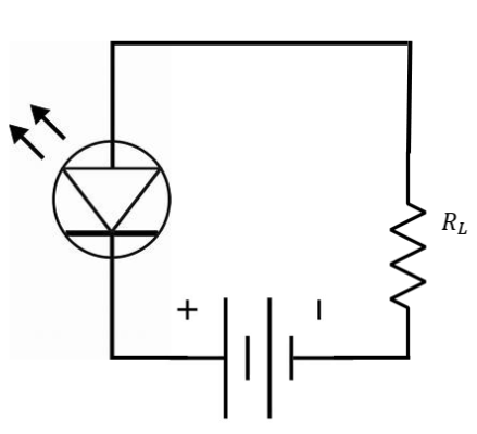
Advantages of LED over incandescent lamps are:
1) They are utilized in numerical displays.
2) It operates at low voltage and has a longer life than glowing bulbs.
4. The input resistance of a silicon transistor is $665\Omega $. Its base current is changed by $15\mu A$, which results in the change in collector current by $2mA$. This transistor is used as a common emitter amplifier with a load resistance of $5k\Omega $. Calculate current gain $({{\beta }_{ac}})$.
Ans:
Given:
$\Delta {{I}_{B}}=15\mu A=15\times {{10}^{-6}}A$
$\Delta {{I}_{C}}=2mA=2\times {{10}^{-3}}A$
\[{{R}_{in}}=665\Omega ,{{R}_{2}}=5k\Omega =5\times {{10}^{3}}\Omega \]
Current gain is given by
${{\beta }_{ac}}=\frac{\Delta {{I}_{c}}}{\Delta {{I}_{B}}}=\frac{2\times {{10}^{-3}}}{15\times {{10}^{-6}}}=133.3$
5. Draw the symbol for Zener diode. Zener diodes have higher dopant densities as compared to ordinary p-n junction diodes. How does it affect the
i. width of the depletion layer?
Ans:
Symbol for Zener diode:
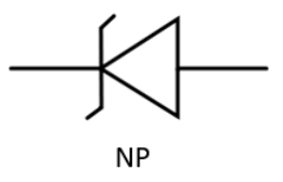
The width of depletion layer of the Zener diode becomes very small due to heavy doping of p and n-regions.
ii. junction field?
Ans.
The junction field of the Zener diode becomes very high due to heavy doping of p and n-regions.
6. A P-N-P transistor is used in common – emitter mode in an amplifier circuit. A change of $40\mu A$ in the base current brings a change of $2mA$ in collector current and $0.04V$ in base – emitter voltage. Find
i. input resistance
Ans:
Given:
$\Delta {{I}_{B}}=40\mu A=40\times {{10}^{-6}}A$
$\Delta {{I}_{C}}=2mA=2\times {{10}^{-3}}A$
$\Delta {{V}_{BE}}=0.04V$
${{R}_{in}}=\frac{\Delta {{V}_{BE}}}{\Delta {{I}_{B}}}=\frac{0.04}{40\times {{10}^{-6}}}=1\times {{10}^{3}}\Omega =1k\Omega $
ii. current amplification factor $(\beta )$ . If a load resistance of $6k\Omega $ is used, then find voltage gain.
Ans.
Current amplification factor is given by
$\beta =\frac{\Delta {{I}_{C}}}{\Delta {{I}_{B}}}=\frac{2\times {{10}^{-3}}}{40\times {{10}^{-6}}}=50$
Here, it is given that load resistance ${{R}_{L}}=6k\Omega $.
Voltage gain is given by
${{A}_{V}}=\beta \frac{{{R}_{L}}}{{{R}_{i}}}=\frac{50\times 6\times {{10}^{3}}}{1\times {{10}^{3}}}=300$
7. A semiconductor has equal electron and whole concentration of $6\times {{10}^{8}}{{m}^{-3}}$ . On doping with certain impurity, electron concentration increases to $8\times {{10}^{12}}{{m}^{-3}}$ .
i. Identify the new semiconductor
Ans:
New semiconductor obtained is N-type as ${{n}_{e}}>{{n}_{h}}$ after doping.
ii. Calculate the new hole concentration.
Ans.
It is known that
${{n}_{e}}{{n}_{h}}={{n}_{i}}^{2}$
Clearly,
${{n}_{h}}=\frac{{{n}_{i}}^{2}}{{{n}_{e}}}=\frac{36\times {{10}^{16}}}{8\times {{10}^{12}}}$
$\Rightarrow {{n}_{h}}=4.5\times {{10}^{4}}{{m}^{-3}}$
iii. How does the energy gap vary with doping?
Ans:
With doping, the energy gap decreases due to generated donor levels in between the valence band and the conduction band.
8. Draw a labelled circuit diagram of a common emitter transistor amplifier. Draw the input and the output wave forms and also state the relation between input and output signal?
Ans:
The circuit diagram of a common emitter transistor amplifier is:
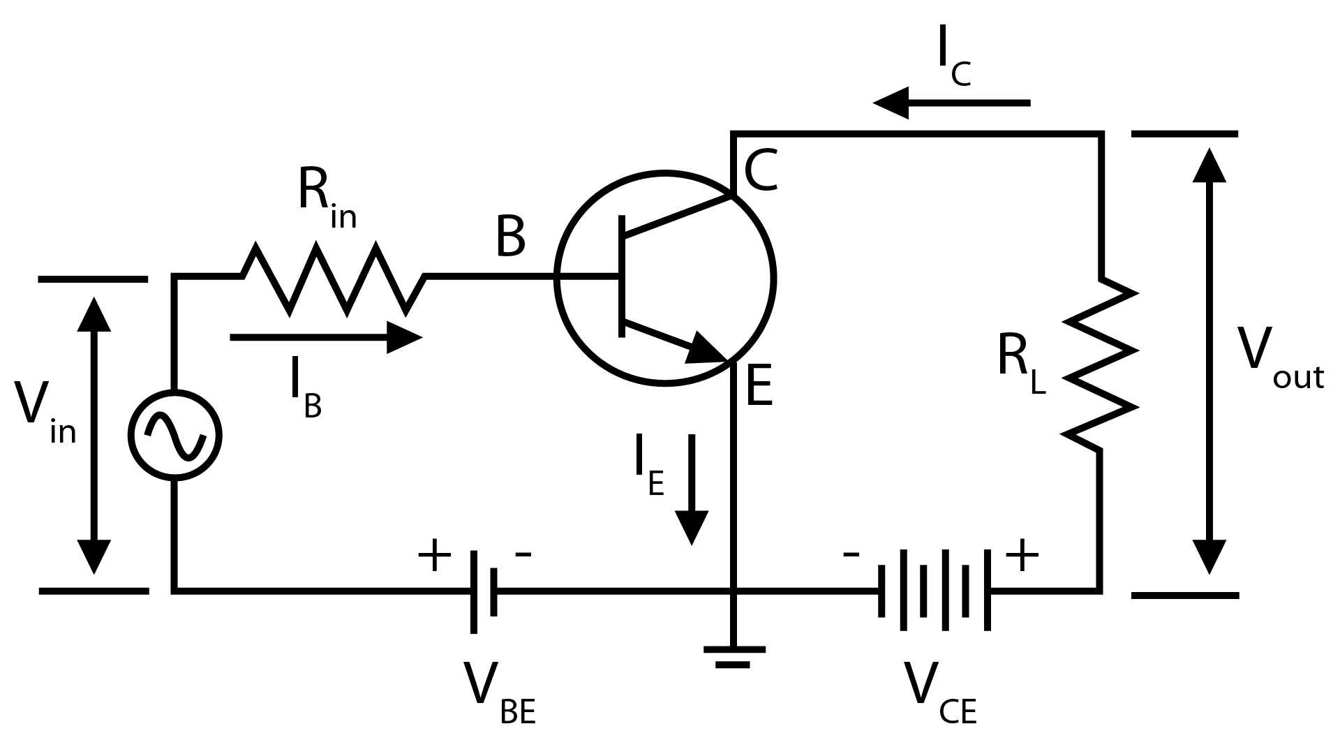
Input wave form is:
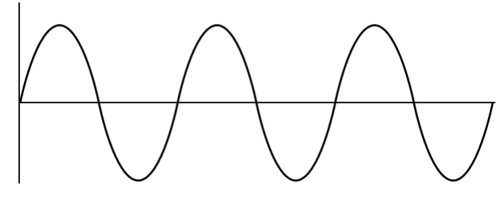
Output wave form is:
There is ${{180}^{\circ }}$ phase difference between output waveform and input waveform.
Also, the output is amplified compared to input waveform.
9. In an intrinsic semiconductor the energy gap ${{E}_{g}}$ is $1.2eV$. Its hole mobility is much smaller than electron mobility and independent of temperature. What is the ratio between conductivity at $600k$ and that at $300k$? Assume that the temperature dependence of intrinsic carrier concentration ${{n}_{i}}$ is given by ${{n}_{i}}={{n}_{o}}\exp \left[ -\frac{{{E}_{g}}}{2{{k}_{B}}T} \right]$ where ${{n}_{o}}$ is a constant.
Ans:
Given:
Energy gap of the given intrinsic semiconductor, ${{E}_{g}}=1.2eV$ .
The temperature dependence of the intrinsic carrier-concentration is given by: ${{n}_{i}}={{n}_{o}}\exp \left[ -\frac{{{E}_{g}}}{2{{k}_{B}}T} \right]$
Where ${{k}_{B}}=\text{Boltzmann constant}=8.62\times {{10}^{-5}}\text{eV }{{\text{K}}^{-1}}$
$T=\text{Temperature}$
${{n}_{o}}=\text{Constant}$
Initial temperature, ${{T}_{1}}=300k$
The intrinsic carrier-concentration at initial temperature is given as:
${{n}_{{{T}_{1}}}}={{n}_{o}}\exp \left[ -\frac{{{E}_{g}}}{2{{k}_{B}}\times 300} \right]$ ….. (1)
Final temperature, ${{T}_{2}}=600k$
The intrinsic carrier-concentration at final temperature is given as: ${{n}_{{{T}_{2}}}}={{n}_{o}}\exp \left[ -\frac{{{E}_{g}}}{2{{k}_{B}}\times 600} \right]$ ….. (2)
The ratio between the conductivities at $600K$ and at $300K$ is equal to the ratio between the respective intrinsic carrier-concentrations at these temperatures.
$\Rightarrow \frac{{{n}_{{{T}_{2}}}}}{{{n}_{{{T}_{1}}}}}=\frac{{{n}_{o}}\exp \left[ -\frac{{{E}_{g}}}{2{{k}_{B}}\times 600} \right]}{{{n}_{o}}\exp \left[ -\frac{{{E}_{g}}}{2{{k}_{B}}\times 300} \right]}$
$\Rightarrow \frac{{{n}_{{{T}_{2}}}}}{{{n}_{{{T}_{1}}}}}=\exp \frac{{{E}_{g}}}{2{{k}_{B}}}\left[ \frac{1}{300}-\frac{1}{600} \right]$
$\Rightarrow \frac{{{n}_{{{T}_{2}}}}}{{{n}_{{{T}_{1}}}}}=\exp \frac{1.2}{2\times 8.62\times {{10}^{-5}}}\left[ \frac{2-1}{600} \right]=\exp [11.6]=1.09\times {{10}^{5}}$
Therefore, the ratio between the conductivities is $1.09\times {{10}^{5}}$.
10. In a p-n junction diode, the current I can be expressed as \[I={{I}_{o}}\exp \left[ \frac{eV}{{{k}_{B}}T}-1 \right]\] where ${{I}_{o}}$ is called the reverse saturation current, $V$ is the voltage across the diode and is positive for forward bias and negative for reverse bias, and $I$ is the current through the diode, ${{k}_{B}}$is the Boltzmann constant ($8.6\times {{10}^{-5}}eV{{K}^{-1}}$) and $T$ is the absolute temperature. If for a given diode${{I}_{o}}=5\times {{10}^{-12}}A$ and $T=300K$, then
a) What will be the forward current at a forward voltage of $0.6V$?
Ans:
In a p-n junction diode, the current’s expression is given as:
\[I={{I}_{o}}\exp \left[ \frac{eV}{{{k}_{B}}T}-1 \right]\]
Where,${{I}_{o}}=\text{Reverse saturation current}=5\times {{10}^{-12}}A$
$T=\text{Absolute temperature}=300K$
${{k}_{B}}=\text{Boltzmann constant}=8.6\times {{10}^{-5}}eV{{K}^{-1}}=1.376\times {{10}^{-23}}J{{K}^{-1}}$
$V=\text{Voltage across the diode}$
Forward voltage $V=0.6V$
$\therefore \text{current, }I=5\times {{10}^{-12}}\left[ \exp \left( \frac{1.6\times {{10}^{-19}}\times 0.6}{1.376\times {{10}^{-23}}\times 300}-1 \right) \right]$
$I=5\times {{10}^{-12}}\times \exp [22.36]=0.0256A$
Therefore, the forward current is about $0.0256A$
b) What will be the increase in the current if the voltage across the diode is increased to $0.7V$?
Ans.
For forward voltage,$V=0.7V$:
$I'=5\times {{10}^{-12}}\left[ \exp \left( \frac{1.6\times {{10}^{-19}}\times 0.7}{1.376\times {{10}^{-23}}\times 300} \right)-1 \right]$
$I'=5\times {{10}^{-12}}\times \exp [26.25]=1.257A$
Hence, the increase in current $\Delta I=I'-I$
$=1.257-0.0256=1.23A$
c) What is the dynamic resistance?
Ans.
Dynamic resistance$=\frac{\text{Change in voltage}}{\text{Change in current}}$
$=\frac{0.7-0.6}{1.23}=\frac{0.1}{1.23}=0.081\Omega $
d) What will be the current if reverse bias voltage changes from $1V$ to $2V$?
Ans.
If the reverse bias voltage varies from $1V$ to $2V$, then the current \[\left( I \right)\] will be equal to ${{I}_{o}}$ in both cases. Therefore, the reverse bias’s dynamic resistance will be infinite.
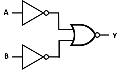
11. You are given the two circuits as shown in Fig. 14.44. Show that circuit
a) acts as OR gate
Ans:
$A$ and $B$ are the inputs and $Y$ is the output of the given circuit.
The left half acts as the NOR Gate while the right half of the given figure acts as the NOT Gate. This is shown in the following figure.
Hence, the output of the NOR Gate $=\overline{A+B}$
This will be the input for the NOT Gate.
Its output will be $\overline{\overline{A+B}}=A+B$
$\therefore Y=A+B$
Hence, this circuit acts as an OR Gate.
b) acts as AND gate.
Ans.
$A$ and $B$ are the inputs and $Y$ is the output of the circuit.
It can be seen from the given figure that the inputs of the NOR Gate at the right half are the outputs of the two NOT Gates.
Hence, the output of the given circuit can be written as:
\[Y=\overline{\overline{A}+\overline{B}}=\overline{\overline{A}}.\overline{\overline{B}}=A.B\]
Hence, this circuit functions as an AND Gate.
12. Write the truth table for the circuits given in Fig. 14.48 consisting of NOR gates only. Identify the logic operations (OR, AND, NOT) performed by the two circuits.
a)
Ans:
$A$ themselves are the two inputs of the NOR gate, and $Y$ is the output.
Hence, the output of the following circuit is $\overline{A+A}$ .
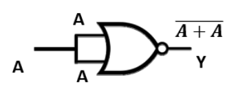
Output $Y=\overline{A+A}=\overline{A}.\overline{A}=\overline{A}$
The truth table for the same is given as:
b)
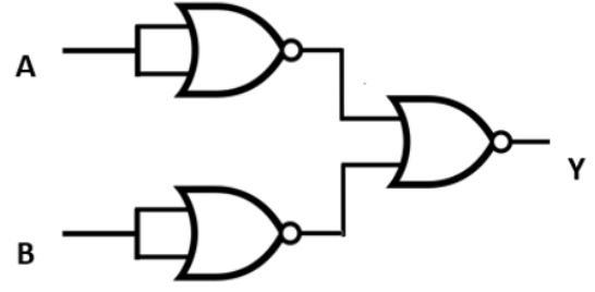
Ans.
$A$ and $B$ are the two inputs and $Y$ is the output of the circuit.
By utilizing the result obtained in solution (a), we can see that the outputs of the given first two NOR gates are $\overline{A}$ and $\overline{B}$, as in the figure given below.
$\overline{A}$ and $\overline{B}$ are the inputs of the last NOR gate. Hence, the output for the circuit will be:
\[Y=\overline{\overline{A}+\overline{B}}=\overline{\overline{A}}.\overline{\overline{B}}=A.B\]
The truth table is:
It is the truth table of an AND gate. Hence, the circuit acts as an AND gate.
Important Formulas from Class 12 Physics Chapter 14 Semiconductor Electronic Material Devices and Simple Circuits
Conductivity of a Semiconductor:
$σ=q(neμe+nhμh)\sigma = q (n_e \mu_e + n_h \mu_h)σ=q(neμe+nhμh)$Resistivity of a Semiconductor:
$ρ=1σ\rho = \frac{1}{\sigma}ρ=σ1$Drift Velocity:
$vd=InqAv_d = \frac{I}{nqA}vd=nqAI$Current in a p-n Junction Diode:
$I=I0(eqVkT−1)I = I_0 \left( e^{\frac{qV}{kT}} - 1 \right)I=I0(ekTqV−1)$Depletion Region Width in p-n Junction:
$W=2ϵrϵ0q(Vb+V)Na+NdW = \sqrt{\frac{2 \epsilon_r \epsilon_0}{q} \frac{(V_b + V)}{N_a + N_d}}W=q2ϵrϵ0Na+Nd(Vb+V)$Current Gain in Transistors:
$β=IcIb\beta = \frac{I_c}{I_b}β=IbIc$Logic Gate Outputs (e.g., AND Gate):
$Y=A⋅BY = A \cdot BY=A⋅B$Cutoff Frequency of Transistor:
$fT=Ic2πCf_T = \frac{I_c}{2\pi C}fT=2πCIc$Rectification Efficiency:
$η=PdcPac\eta = \frac{P_{dc}}{P_{ac}}η=PacPdc$
Benefits of Class 12 Physics Chapter 14 Semiconductor Electronic Material Devices and Simple Circuits
Chapter 14 of Class 12 Physics gives a detailed explanation about Semiconductors, n-type, and P-type semiconductors.
In this chapter, we mainly focused on definitions and meanings of minority charge carriers and majority charge carriers.
We learn about the different types of materials like conductors, insulators, and semiconductors. We come across the concept of the energy gap.
The method of doping, the importance of doping, a different type of dopants used in semiconductors is also covered in this chapter.
Different types of diodes like Pn-junction diodes, Zener diodes, etc… are studied along with their characteristics.
Tips to Study Class 12 Physics Chapter 14 Important Questions
Understand the properties of semiconductors and their types (intrinsic and extrinsic).
Memorize key formulas and their derivations for numerical problems.
Focus on the working principles of diodes, transistors, and logic gates.
Solve NCERT exercises and additional questions from reference books.
Practice drawing and analyzing circuit diagrams for clarity.
Study the practical applications of semiconductor devices in real-world scenarios.
Revise Boolean algebra for a better understanding of logic gates.
Related Study Materials for CBSE Class 12 Physics Chapter 14
Conclusion
Semiconductor Electronics is an exciting and essential chapter 14 that bridges physics and practical electronics. By mastering the concepts and formulas, students can crack board exams and competitive tests. Utilise the Vedantu FREE PDF of important questions, practice diligently, and build a strong foundation in modern electronics!
Download CBSE Class 12 Physics Important Questions 2026-27 PDF
CBSE Class 12 Physics Chapter-wise Important Questions and Answers cover topics from all other chapters, helping students prepare thoroughly by focusing on key topics for easier revision.
Additional Study Materials for Class 12 Physics

FAQs on Important Questions For Class 12 Physics Chapter 14 Semiconductor Electronic Material Devices And Simple Circuits - 2026-27
1. What are the most important topics in Chapter 14, Semiconductor Electronics, for the CBSE Class 12 board exam 2026-27?
For the CBSE Class 12 board exam, the most important topics from this chapter include:
- Energy Bands: Differentiating between conductors, insulators, and semiconductors.
- Semiconductor Types: Intrinsic vs. Extrinsic, p-type vs. n-type, and the concept of doping.
- p-n Junction Diode: Formation, biasing (forward and reverse), and V-I characteristics.
- Diode Applications: Working principles of Half-wave and Full-wave rectifiers.
- Special Purpose Diodes: Zener diode as a voltage regulator, Photodiode, and LED.
- Transistors: Basic action, characteristics of a CE amplifier, and its use as a switch.
- Logic Gates: Understanding the operation and truth tables for AND, OR, NOT, NAND, and NOR gates.
2. How can we distinguish between conductors, insulators, and semiconductors using the energy band theory?
Based on the energy band theory, these materials are distinguished by the energy gap (Eg) between their valence and conduction bands:
- In conductors, the valence band and conduction band overlap, so there is no energy gap. This allows electrons to move freely, resulting in high conductivity.
- In insulators, there is a very large energy gap (Eg > 3 eV) between the valence and conduction bands. Electrons cannot easily jump to the conduction band, making them poor conductors of electricity.
- In semiconductors, the energy gap is small (Eg < 3 eV). At room temperature, some electrons gain enough thermal energy to jump to the conduction band, allowing for moderate conductivity which can be controlled by doping.
3. What is a p-n junction? Explain the formation of the depletion region and potential barrier.
A p-n junction is formed when a p-type semiconductor is brought into close contact with an n-type semiconductor. During its formation, electrons from the n-region diffuse to the p-region, and holes from the p-region diffuse to the n-region due to the concentration gradient. This diffusion creates an area near the junction that is depleted of free charge carriers, known as the depletion region. The accumulation of immobile positive ions in the n-region and negative ions in the p-region sets up an electric field and a potential difference across the junction. This potential difference, which opposes further diffusion of charge carriers, is called the potential barrier.
4. Explain the working of a full-wave rectifier and state its output frequency for a 50 Hz input AC signal.
A full-wave rectifier converts both halves of an AC input signal into a pulsating DC output. It typically uses two diodes and a center-tapped transformer.
- During the positive half-cycle of the AC input, diode D1 is forward-biased and conducts, while D2 is reverse-biased and does not. Current flows through the load resistor.
- During the negative half-cycle, diode D2 becomes forward-biased and conducts, while D1 is reverse-biased. Current again flows through the load resistor in the same direction.
Since both halves of the input cycle are utilised, the output frequency is twice the input frequency. For an input of 50 Hz, the output frequency of a full-wave rectifier will be 100 Hz.
5. What is the fundamental difference between forward biasing and reverse biasing of a p-n junction diode?
The fundamental difference lies in the connection to the voltage source and its effect on the depletion region:
- Forward Biasing: The p-type region is connected to the positive terminal and the n-type region to the negative terminal of the battery. This applied voltage opposes the potential barrier, reducing the width of the depletion region and allowing a large current to flow due to majority charge carriers. The diode offers very low resistance.
- Reverse Biasing: The p-type region is connected to the negative terminal and the n-type region to the positive terminal. This applied voltage supports the potential barrier, increasing the width of the depletion region and blocking the flow of majority carriers. Only a very small current (due to minority carriers) flows, and the diode offers very high resistance.
6. Describe the V-I characteristics of a Zener diode and explain its role as a voltage regulator.
The V-I characteristics of a Zener diode are similar to a normal p-n junction diode in forward bias. However, in reverse bias, it exhibits a controlled breakdown at a specific voltage called the Zener voltage (Vz). After this breakdown, the voltage across the diode remains nearly constant even as the current changes significantly. This property allows it to be used as a voltage regulator. When connected in reverse bias across a fluctuating voltage source, it maintains a constant output voltage equal to Vz across the load, absorbing any excess voltage.
7. A transistor has a current amplification factor (β) of 100 and a base current (IB) of 20µA. For a common-emitter configuration, calculate the collector current (IC) and emitter current (IE).
The calculations are as follows:
1. To find Collector Current (IC):
The current amplification factor (β) is given by the formula β = IC / IB.
Therefore, IC = β × IB = 100 × 20 µA = 2000 µA or 2 mA.
2. To find Emitter Current (IE):
The emitter current is the sum of the base current and the collector current: IE = IB + IC.
IE = 20 µA + 2000 µA = 2020 µA or 2.02 mA.
8. What are the most important types of numerical problems from the Semiconductors chapter for the Class 12 Physics exam?
For the Class 12 exam, you should focus on numericals based on:
- Doping and Carrier Concentration: Calculating electron and hole concentrations in doped semiconductors using the law of mass action (nenh = ni2).
- Transistor Parameters: Problems involving current gain (α and β), emitter, base, and collector currents (IE = IB + IC), and voltage/power gain in amplifiers.
- Diode Equation: Calculating forward current or dynamic resistance using the diode current equation.
- Photodiode and Band Gap Energy: Determining if a photodiode can detect a specific wavelength of light based on its band gap energy (E = hc/λ).
9. Explain why the base region of a transistor must be very thin and lightly doped for effective amplification.
The base region of a transistor is made thin and lightly doped to ensure most of the charge carriers from the emitter pass through to the collector.
- Thin Base: A thin base region reduces the transit time for charge carriers, minimising the chance for them to recombine with the majority carriers in the base. This ensures a high collector current.
- Light Doping: A low concentration of majority carriers in the base means there are fewer carriers available for recombination with the injected emitter carriers. This results in a very small base current (IB) and a large collector current (IC), which is essential for achieving a high current amplification factor (β = IC/IB).
10. A photodiode is fabricated from a semiconductor with a band gap of 2.0 eV. Can it detect light of wavelength 6000 Å? Justify your answer with calculations.
Yes, the photodiode can detect this light. Here's the justification:
1. First, calculate the energy (E) of the incident light using the formula E = hc/λ.
- Wavelength, λ = 6000 Å = 6000 × 10-10 m
- Planck's constant, h ≈ 6.63 × 10⁻³⁴ J·s
- Speed of light, c = 3 × 10⁸ m/s
2. Substitute the values: E = (6.63 × 10-34 × 3 × 108) / (6000 × 10-10) J ≈ 3.315 × 10⁻¹⁹ J.
3. Convert this energy to electron volts (eV) by dividing by 1.6 × 10⁻¹⁹ J/eV: E ≈ 3.315 × 10⁻¹⁹ / 1.6 × 10⁻¹⁹ ≈ 2.07 eV.
4. Conclusion: For a photodiode to detect light, the energy of the incident photons (E) must be greater than or equal to the semiconductor's band gap (Eg). Since the incident light's energy (2.07 eV) is greater than the band gap (2.0 eV), the photodiode can absorb the photon and generate an electron-hole pair, thus detecting the signal.
11. In a common-emitter (CE) amplifier, why is the output voltage 180° out of phase with the input voltage?
This 180° phase reversal in a CE amplifier occurs due to the way the circuit operates. The output voltage is measured at the collector (VCE), which is given by the equation VCE = VCC - ICRC, where VCC is the supply voltage and RC is the collector resistor. When a positive half-cycle of the input AC signal is applied to the base, the forward bias of the emitter-base junction increases. This causes a large increase in the collector current (IC). As IC increases, the voltage drop across RC (ICRC) also increases. Consequently, the output voltage VCE decreases. This means a positive input signal results in a negative-going output signal, creating the 180° phase shift.
12. How do you identify the logic operation performed by a combination of basic logic gates, for example, the output of a NAND gate fed into a NOT gate?
To identify the logic operation, you should trace the Boolean expression step-by-step.
For the given example (NAND followed by NOT):
- Let the inputs be A and B.
- The output of the NAND gate is Y1 = (A.B)'.
- This output Y1 is then fed into a NOT gate.
- The final output Y will be the negation of Y1, so Y = (Y1)' = ((A.B)')'.
Using De Morgan's theorems or the property of double negation ((X)')' = X, we find that Y = A.B. This Boolean expression corresponds to the AND gate. Therefore, the combination performs the function of an AND gate.
13. If a pure silicon crystal is doped simultaneously with an equal concentration of Arsenic (pentavalent) and Indium (trivalent) atoms, what type of semiconductor will it become?
The resulting semiconductor will behave almost like an intrinsic (pure) semiconductor. This is because the pentavalent Arsenic atoms are donors, providing extra electrons, while the trivalent Indium atoms are acceptors, creating holes. When their concentrations are equal, each free electron donated by an Arsenic atom will be captured by a hole created by an Indium atom. This process, known as compensation, effectively neutralizes the effect of both dopants, leaving the charge carrier concentration nearly equal to that of a pure semiconductor.