


The transfer characteristics of a transistor means a plot of:
A. Input voltage versus input current
B. Output voltage versus output current
C. Input voltage versus output voltage
D. Input current versus output current
Answer
598.8k+ views
Hint: Transfer characteristics for an electrical component or instrument is a curve that shows how variation in an input quantity in the electronic circuit affects the output quantity.
Complete step by step answer:
A transistor is a three terminal device made up of semiconductor materials like Silicon and Germanium (4 electrons in valence shell). It has 3 regions namely: emitter, base and a collector based on the amount of doping of the material.
Doping of a material is known as adding a different element to the semiconductor material in order to create n type and p type material. N type material has free electrons, therefore elements with more electrons in the valence shell than the semiconductors are added, for example Phosphorous (5 electrons in valence shell). Similarly, for P type, there is abundance of holes or lack of electrons, that is where the electrons get attracted to (one can think of the nature similar to positive charge, thus the name p type). One of the examples of elements added is Boron (3 electrons in valence shell).
Transistors have two main types n-p-n and p-n-p and there are 3 configurations of transistors: Common-Emitter, common base and common collector transistor.
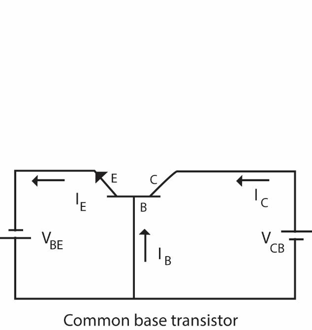
Let us consider one the most used configuration, common-base, to answer the question. In a common base transistor, the base emitter junction makes up the input side and the base collector junction makes the output terminal of the transistor.
If we consider their transfer characteristics of a Common-Base transistor it would be a plot between the Emitter base voltage ${{V}_{BE}}$ and the Base Collector voltage ${{V}_{BC}}$ .
The following is the diagram of a transistor in a common base configuration.
Similarly, for Common emitter or a common collector configuration the transfer characteristics would be a plot between the input voltage and output voltage.
So, the correct answer is option C. input voltage versus output voltage.
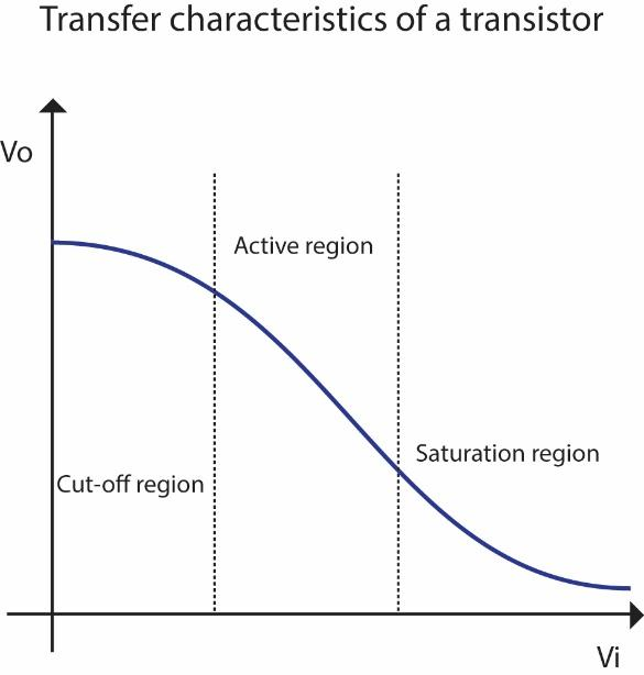
The following graph shows the transfer function for a transistor. The working is in 3 modes as mentioned.
Note: Apart from transfer characteristics there are Input characteristics and output characteristics of a transistor. The input characteristic is a curve between input current and input voltage keeping the output voltage constant. And the output characteristics is a plot between output current and output voltage keeping input current constant.
Students should note that in plotting the transfer characteristics the input signal is typically represented on the x-axis and the output signal on the y-axis.
Complete step by step answer:
A transistor is a three terminal device made up of semiconductor materials like Silicon and Germanium (4 electrons in valence shell). It has 3 regions namely: emitter, base and a collector based on the amount of doping of the material.
Doping of a material is known as adding a different element to the semiconductor material in order to create n type and p type material. N type material has free electrons, therefore elements with more electrons in the valence shell than the semiconductors are added, for example Phosphorous (5 electrons in valence shell). Similarly, for P type, there is abundance of holes or lack of electrons, that is where the electrons get attracted to (one can think of the nature similar to positive charge, thus the name p type). One of the examples of elements added is Boron (3 electrons in valence shell).
Transistors have two main types n-p-n and p-n-p and there are 3 configurations of transistors: Common-Emitter, common base and common collector transistor.
Let us consider one the most used configuration, common-base, to answer the question. In a common base transistor, the base emitter junction makes up the input side and the base collector junction makes the output terminal of the transistor.
If we consider their transfer characteristics of a Common-Base transistor it would be a plot between the Emitter base voltage ${{V}_{BE}}$ and the Base Collector voltage ${{V}_{BC}}$ .
The following is the diagram of a transistor in a common base configuration.
Similarly, for Common emitter or a common collector configuration the transfer characteristics would be a plot between the input voltage and output voltage.
So, the correct answer is option C. input voltage versus output voltage.
The following graph shows the transfer function for a transistor. The working is in 3 modes as mentioned.
Note: Apart from transfer characteristics there are Input characteristics and output characteristics of a transistor. The input characteristic is a curve between input current and input voltage keeping the output voltage constant. And the output characteristics is a plot between output current and output voltage keeping input current constant.
Students should note that in plotting the transfer characteristics the input signal is typically represented on the x-axis and the output signal on the y-axis.
Recently Updated Pages
Master Class 12 Economics: Engaging Questions & Answers for Success
Master Class 12 Physics: Engaging Questions & Answers for Success
Master Class 12 English: Engaging Questions & Answers for Success
Master Class 12 Social Science: Engaging Questions & Answers for Success
Master Class 12 Maths: Engaging Questions & Answers for Success
Master Class 12 Business Studies: Engaging Questions & Answers for Success
Trending doubts
Which are the Top 10 Largest Countries of the World?
What are the major means of transport Explain each class 12 social science CBSE
Draw a labelled sketch of the human eye class 12 physics CBSE
Why cannot DNA pass through cell membranes class 12 biology CBSE
Differentiate between insitu conservation and exsitu class 12 biology CBSE
Draw a neat and well labeled diagram of TS of ovary class 12 biology CBSE