


Explain the working of P-N junction diodes in forward and reverse biased mode.
Answer
569.4k+ views
Hint: The main difference between the forward biasing and the reverse biasing of the junction will be according to the direction of applied external voltage. The direction of the external voltage in reverse biasing will be opposite to the external voltage in forward biasing. The passage of current in the forward basing will be lower than that of the reverse biasing.
Complete step by step answer:
A p-n junction is a junction that is also known as boundary or interference between two types of semiconductor materials that is inside a single crystal of semiconductor.
P-N JUNCTION IN FORWARD BIASED: in the case of forward biasing of a p-n junction, the p-type semiconductor will be connected to the positive terminal of the battery whereas n-type semiconductor will be connected to the negative terminal of the battery.
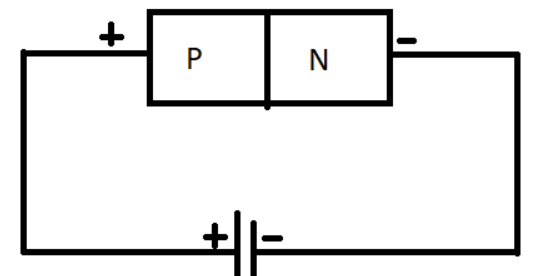
In this type of semiconductor, the electrons from the negative terminal of the battery will move to the n-type of the semiconductor. These electrons will move towards p-type of semiconductor and combine with the holes. These combined electrons will move toward the positive terminal of the battery which results in development of more free holes that will move to the n-type of the semiconductor. This will result in the decrease in the potential barrier with the decrease in depletion layer.
P-N JUNCTION IN REVERSE BIASED: in the case of reverse biasing of the p-n junction, the p-type semiconductor will be connected to the negative terminal of the battery whereas the n-type semiconductor will be connected to the positive terminal of the battery.
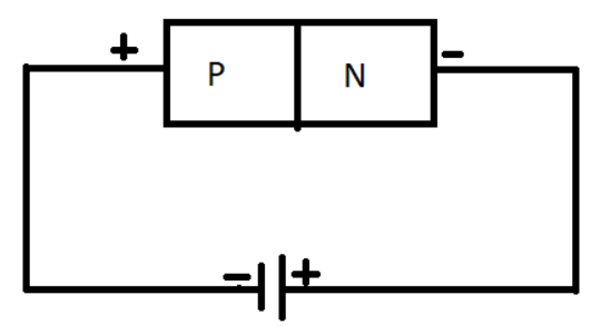
In this type of semiconductor, the electrons from the n-type semiconductor will get attracted by the battery and the holes from the positive terminal of the battery will move towards the n-type. On the other hand, the holes from the p-type semiconductor will get attracted by the negative terminal of the battery and the electrons from the negative terminal of the battery will move towards the p-type semiconductor. This results in the increase in potential barrier that results in the expansion of the depletion layer.
Note:
The decrease in the depletion layer, in the case of forward biasing, the current will pass through the diode. This is because the resistance in this case will be lower.
Also, in the case of reverse biasing, the current will not pass through the diode because the resistance will increase with the expansion of the depletion layer.
Complete step by step answer:
A p-n junction is a junction that is also known as boundary or interference between two types of semiconductor materials that is inside a single crystal of semiconductor.
P-N JUNCTION IN FORWARD BIASED: in the case of forward biasing of a p-n junction, the p-type semiconductor will be connected to the positive terminal of the battery whereas n-type semiconductor will be connected to the negative terminal of the battery.
In this type of semiconductor, the electrons from the negative terminal of the battery will move to the n-type of the semiconductor. These electrons will move towards p-type of semiconductor and combine with the holes. These combined electrons will move toward the positive terminal of the battery which results in development of more free holes that will move to the n-type of the semiconductor. This will result in the decrease in the potential barrier with the decrease in depletion layer.
P-N JUNCTION IN REVERSE BIASED: in the case of reverse biasing of the p-n junction, the p-type semiconductor will be connected to the negative terminal of the battery whereas the n-type semiconductor will be connected to the positive terminal of the battery.
In this type of semiconductor, the electrons from the n-type semiconductor will get attracted by the battery and the holes from the positive terminal of the battery will move towards the n-type. On the other hand, the holes from the p-type semiconductor will get attracted by the negative terminal of the battery and the electrons from the negative terminal of the battery will move towards the p-type semiconductor. This results in the increase in potential barrier that results in the expansion of the depletion layer.
Note:
The decrease in the depletion layer, in the case of forward biasing, the current will pass through the diode. This is because the resistance in this case will be lower.
Also, in the case of reverse biasing, the current will not pass through the diode because the resistance will increase with the expansion of the depletion layer.
Recently Updated Pages
Master Class 12 Economics: Engaging Questions & Answers for Success
Master Class 12 Physics: Engaging Questions & Answers for Success
Master Class 12 English: Engaging Questions & Answers for Success
Master Class 12 Social Science: Engaging Questions & Answers for Success
Master Class 12 Maths: Engaging Questions & Answers for Success
Master Class 12 Business Studies: Engaging Questions & Answers for Success
Trending doubts
Which are the Top 10 Largest Countries of the World?
What are the major means of transport Explain each class 12 social science CBSE
Draw a labelled sketch of the human eye class 12 physics CBSE
Why cannot DNA pass through cell membranes class 12 biology CBSE
Differentiate between insitu conservation and exsitu class 12 biology CBSE
Draw a neat and well labeled diagram of TS of ovary class 12 biology CBSE