


Draw the circuit symbol of the p-n-p transistor.
Answer
584.7k+ views
HintThe transistor in which one n-type material is doped with two p-type materials such a type of transistor is known as a PNP transistor. It is a current controlled device. The small amount of base current controlled both the emitter and collector current. The PNP transistor has two crystal diodes connected back to back. The left side of the diode is known as the emitter-base diode and the right side of the diode is known as the collector-base diode.
Complete step-by-step solution:Definition : A PNP transistor is a bipolar junction transistor constructed by sandwiching an N-type semiconductor between two P-type semiconductors. A PNP transistor has three terminals – a Collector (C), Emitter (E) and Base (B). The PNP transistor behaves like two PN junctions diodes connected back to back.
These back to back PN junction diodes are known as the collector-base junction and base-emitter junction.
Regarding the three terminals of the PNP transistor, the Emitter is a region used to supply charge carriers to the Collector via the Base region. The Collector region collects most of all charge carriers emitted from the Emitter. The Base region triggers and controls the amount of current flows through the Emitter to Collector.
Given below is the symbol of PNP transistor
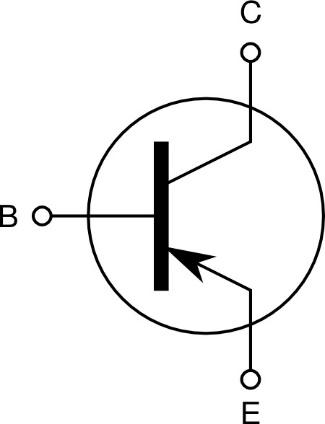
If you apply a Kirchhoff’s current law (KCL), the emitter current is a summation of the base current and collector current.
${I_E} = {I_B} + {I_C}$
Note: One of the major differences between the diode and the transistor is that the diode converts the alternating current into direct current while the transistor transfers the input signals from the low resistance circuit to high resistance circuit. And Diode can’t be controlled through switches while Transistors can be controlled with switches.
Complete step-by-step solution:Definition : A PNP transistor is a bipolar junction transistor constructed by sandwiching an N-type semiconductor between two P-type semiconductors. A PNP transistor has three terminals – a Collector (C), Emitter (E) and Base (B). The PNP transistor behaves like two PN junctions diodes connected back to back.
These back to back PN junction diodes are known as the collector-base junction and base-emitter junction.
Regarding the three terminals of the PNP transistor, the Emitter is a region used to supply charge carriers to the Collector via the Base region. The Collector region collects most of all charge carriers emitted from the Emitter. The Base region triggers and controls the amount of current flows through the Emitter to Collector.
Given below is the symbol of PNP transistor
If you apply a Kirchhoff’s current law (KCL), the emitter current is a summation of the base current and collector current.
${I_E} = {I_B} + {I_C}$
Note: One of the major differences between the diode and the transistor is that the diode converts the alternating current into direct current while the transistor transfers the input signals from the low resistance circuit to high resistance circuit. And Diode can’t be controlled through switches while Transistors can be controlled with switches.
Recently Updated Pages
Master Class 12 Economics: Engaging Questions & Answers for Success
Master Class 12 Physics: Engaging Questions & Answers for Success
Master Class 12 English: Engaging Questions & Answers for Success
Master Class 12 Social Science: Engaging Questions & Answers for Success
Master Class 12 Maths: Engaging Questions & Answers for Success
Master Class 12 Business Studies: Engaging Questions & Answers for Success
Trending doubts
Which are the Top 10 Largest Countries of the World?
What are the major means of transport Explain each class 12 social science CBSE
Draw a labelled sketch of the human eye class 12 physics CBSE
Why cannot DNA pass through cell membranes class 12 biology CBSE
Differentiate between insitu conservation and exsitu class 12 biology CBSE
Draw a neat and well labeled diagram of TS of ovary class 12 biology CBSE