


Explain using a circuit diagram the working of n-p-n transistors as CE amplifiers. Hence obtain expression for its voltage gain in common emitter configuration.
Answer
569.1k+ views
Hint: If we combine two extrinsic semiconductors we get diodes. Extrinsic semiconductor in which electrons are excess are called n-type semiconductor whereas extrinsic semiconductor in which holes are excess are called p-type semiconductor. Now if we combine two diodes we get a transistor. It can be a p-n-p transistor or n-p-n transistor. That transistor has emitter base and collector and can be used as switches, amplifiers and as many other devices
Formula used:
${A_V} = \beta \dfrac{{{R_C}}}{{{R_B}}}$
Complete answer:
The voltage which we applied will be lesser than the output voltage. That means there will be some voltage gain. That voltage gain depends upon the load resistance and the input resistance.
An ideal amplifier will be having high input impedance and very low output impedance. It should not draw any current from the input
Let the output voltage be ${V_0}$ and the input voltage that is being amplified be ${V_i}$
Gain in the amplifier can be given as
$A.G = \dfrac{{{V_0}}}{{{V_i}}}$
That is the ratio of output voltage to the input voltage. The circuit is shown below
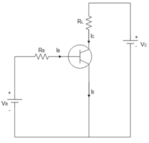
In the above diagram emitter and collector will be n type and base will be p type.
When input base current is passed in the upper half base emitter junction will be in forward bias and then current passing from collector to emitter through base increases. So collector current increases.
When input base current is passed in the lower negative half base emitter junction will be in reverse bias and then current passing from collector to emitter through base decreases. So collector current decreases.
The ratio of this change in collector current to change in base current is current gain and denoted by beta.
$\beta = \dfrac{{\Delta {I_C}}}{{\Delta {I_B}}}$
Ratio of collector resistance to base resistance is $\dfrac{{{R_C}}}{{{R_B}}}$. Product of this ratio and current gain is called voltage gain.
$\eqalign{
& \dfrac{{{V_0}}}{{{V_i}}} = \beta \dfrac{{{R_C}}}{{{R_B}}} \cr
& \therefore \dfrac{{{V_0}}}{{{V_i}}} = \left( {\dfrac{{\Delta {I_C}}}{{\Delta {I_B}}}} \right)\dfrac{{{R_C}}}{{{R_B}}} \cr} $
Note:
The characteristics of emitter, base and collector will be different. Emitter is highly doped while the collector and base are lightly doped. The width of the base is very less. Moreover emitter-base junction is always forward biased whereas base-collector junction is always reverse biased. Forward biased in the sense diode provides very low resistance and reverse biased in the sense diode provides huge resistance.
Formula used:
${A_V} = \beta \dfrac{{{R_C}}}{{{R_B}}}$
Complete answer:
The voltage which we applied will be lesser than the output voltage. That means there will be some voltage gain. That voltage gain depends upon the load resistance and the input resistance.
An ideal amplifier will be having high input impedance and very low output impedance. It should not draw any current from the input
Let the output voltage be ${V_0}$ and the input voltage that is being amplified be ${V_i}$
Gain in the amplifier can be given as
$A.G = \dfrac{{{V_0}}}{{{V_i}}}$
That is the ratio of output voltage to the input voltage. The circuit is shown below
In the above diagram emitter and collector will be n type and base will be p type.
When input base current is passed in the upper half base emitter junction will be in forward bias and then current passing from collector to emitter through base increases. So collector current increases.
When input base current is passed in the lower negative half base emitter junction will be in reverse bias and then current passing from collector to emitter through base decreases. So collector current decreases.
The ratio of this change in collector current to change in base current is current gain and denoted by beta.
$\beta = \dfrac{{\Delta {I_C}}}{{\Delta {I_B}}}$
Ratio of collector resistance to base resistance is $\dfrac{{{R_C}}}{{{R_B}}}$. Product of this ratio and current gain is called voltage gain.
$\eqalign{
& \dfrac{{{V_0}}}{{{V_i}}} = \beta \dfrac{{{R_C}}}{{{R_B}}} \cr
& \therefore \dfrac{{{V_0}}}{{{V_i}}} = \left( {\dfrac{{\Delta {I_C}}}{{\Delta {I_B}}}} \right)\dfrac{{{R_C}}}{{{R_B}}} \cr} $
Note:
The characteristics of emitter, base and collector will be different. Emitter is highly doped while the collector and base are lightly doped. The width of the base is very less. Moreover emitter-base junction is always forward biased whereas base-collector junction is always reverse biased. Forward biased in the sense diode provides very low resistance and reverse biased in the sense diode provides huge resistance.
Recently Updated Pages
Master Class 12 Economics: Engaging Questions & Answers for Success
Master Class 12 Physics: Engaging Questions & Answers for Success
Master Class 12 English: Engaging Questions & Answers for Success
Master Class 12 Social Science: Engaging Questions & Answers for Success
Master Class 12 Maths: Engaging Questions & Answers for Success
Master Class 12 Business Studies: Engaging Questions & Answers for Success
Trending doubts
Which are the Top 10 Largest Countries of the World?
What are the major means of transport Explain each class 12 social science CBSE
Draw a labelled sketch of the human eye class 12 physics CBSE
Why cannot DNA pass through cell membranes class 12 biology CBSE
Differentiate between insitu conservation and exsitu class 12 biology CBSE
Draw a neat and well labeled diagram of TS of ovary class 12 biology CBSE